
Electronic PCB Boards Impact the Internet of Things IoT Landscape
The Internet of Things, or IoT, is changing the way we live. While many consumers think of smartphones, IoT is extending beyond mobile devices to incorporate everyday household items and industrial machinery. Regardless of the industry, IoT requires reliable and fast connectivity to streamline operations on a large scale. This is where PCB technology leaves its mark.
PCBs are a critical part of the IoT landscape, and it’s essential to know how they impact the longevity of IoT equipment. In addition to enabling high-speed data transmission, PCBs also help to maintain the integrity of sensitive electronics in diverse environments. Using specific PCB design software, manufacturers can minimize the risks of signal interference and electromagnetic emissions while also ensuring proper functionality.
When designing electronic pcb board, there are several key factors to consider, including the material and construction, the size, and the type of assembly. Choosing the best materials and integrating protective coatings can help minimize environmental damage to the circuit board, increasing its durability. These coatings can also prevent corrosion in harsh environments.
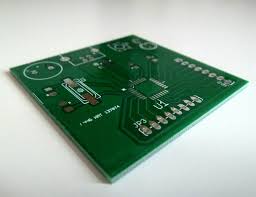
How Do Electronic PCB Boards Impact the Internet of Things IoT Landscape?
In addition, utilizing flexible PCBs is an excellent choice for IoT designs because of their ability to conform to irregular shapes and fit into tight spaces. This flexibility allows them to adapt easily to the unpredictable form factor of IoT products without sacrificing long-term reliability. Compared to rigid PCBs, flexible ones are more durable and can resist extreme temperatures, humidity, and corrosive chemicals.
Another important consideration when designing IoT PCBs is the layout of components. Using a flexible layout can save space and reduce the amount of wires that need to be routed through the circuit board. It can also simplify the manufacturing process and make it more cost-effective.
Lastly, PCB designers must pay close attention to power consumption and battery life when creating IoT devices. This is because IoT devices require high levels of functionality and connectivity, resulting in a higher power consumption. Using the latest PCB design techniques, manufacturers can maximize space utilization and reduce power consumption.
A good example of this is the use of High-Density Interconnect (HDI) technology, which enables increased component density and finer trace routing, making it easier to create compact IoT devices. This helps to increase the longevity of IoT products by reducing their power consumption and battery usage.
Having an intimate understanding of how IoT PCBs impact the longevity and functionality of connected devices is vital for all manufacturers. PCBs play an important role in the IoT landscape and are a key element of connectivity, so it’s essential to keep up with the latest trends in PCB design and manufacture. By doing so, manufacturers can ensure that their IoT equipment is compatible with other systems and provides optimal performance. Ultimately, this will allow for greater efficiency and productivity on a global scale.