
How do you solder components onto a printed circuit board and assembly?
solder components onto a printed circuit board and assembly
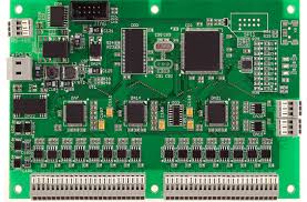
Soldering components onto a printed circuit board (PCB) and assembly is a fundamental skill in electronics manufacturing and assembly processes. Whether you’re a hobbyist assembling a DIY project or a professional engineer manufacturing electronic devices, understanding the principles and techniques of soldering is essential for achieving reliable and robust connections. From selecting the right tools and materials to mastering soldering techniques, here’s a comprehensive guide on how to solder components onto a PCB and assembly.
The first step in soldering components onto a printed circuit board and assembly is to prepare the board and components. This involves ensuring that the PCB is clean and free of any debris, oxidation, or contamination that could affect soldering quality. Components should be carefully inspected for defects or damage, and their leads or pads should be properly aligned and trimmed if necessary.
Next, it’s essential to select the appropriate soldering equipment and materials. A soldering iron with the right wattage and tip size for the job is crucial, as is high-quality solder wire with the appropriate flux core and diameter. Additionally, soldering aids such as flux pens, solder wick, and soldering flux may be used to enhance soldering performance and ensure clean, reliable joints.
How do you solder components onto a printed circuit board and assembly?
Before soldering, it’s recommended to apply flux to the pads on the PCB and the leads of the components. Flux helps remove oxidation and promotes solder flow, resulting in strong, reliable solder joints. Flux can be applied using a flux pen or brush, or it may be included in the solder wire itself. Applying flux ensures proper wetting and adhesion of the solder to the surfaces being soldered.
Once the PCB and components are prepared, the soldering process can begin. To solder a component onto a PCB, place the component onto the corresponding pads on the board, ensuring that the leads are correctly aligned and making good contact with the pads. Hold the component in place with tweezers or a PCB holder to prevent movement during soldering.
With the component in position, heat the soldering iron to the appropriate temperature and apply heat to the joint area. The soldering iron should be held at a slight angle to the joint, allowing the tip to contact both the pad and the component lead simultaneously. Once the joint reaches the appropriate temperature, touch the solder wire to the joint, allowing the solder to flow and form a smooth, shiny fillet.
It’s essential to apply the right amount of solder to achieve a reliable joint. Too little solder may result in a weak or incomplete joint, while too much solder can lead to bridging or shorts between adjacent pads. The goal is to create a concave fillet that covers the entire joint area without excess buildup or irregularities.
After soldering, inspect the joints carefully to ensure they are clean, shiny, and free of defects such as cold solder joints, bridges, or voids. Use a magnifying glass or microscope if necessary to examine the joints closely. Any defects should be corrected immediately using solder wick or a solder sucker to remove excess solder and reflow the joint as needed.
Finally, it’s essential to clean the PCB after soldering to remove any flux residue or contaminants that may remain. This can be done using a flux remover spray or isopropyl alcohol and a brush or swab. Proper cleaning ensures the integrity and reliability of the solder joints and prevents corrosion or damage to the PCB over time.
In conclusion, soldering components onto a printed circuit board and assembly is a fundamental skill in electronics manufacturing and assembly processes. By following the principles and techniques outlined in this guide and practicing proper soldering procedures, individuals can achieve reliable, high-quality solder joints that ensure the performance and reliability of electronic devices.