
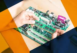
Bridging During PCB SMT Assembly
There’s a lot to consider when you’re working on a PCB assembly project. There are the different technologies involved (through-hole, surface mount, and mixed), the components themselves, and the manufacturing process that will be employed. It’s important to be aware of the steps that need to be taken with each technology in order to ensure success.
One of the key steps that needs to be taken during pcb smt assembly is applying solder paste. Solder bridges can occur for a number of reasons, including insufficient solder paste volume, incorrect or misaligned stencil design, or improper reflow solder joint reflow. Solder bridges can be costly, as they often require a human operator to rework the part in question, which can add up in terms of labor costs and lost production time.
As the electronics industry continues to shrink, it’s become increasingly difficult to cram in the same amount of technology that was once housed in a tower desktop into something that can fit on your wrist. While this is a good thing for consumers, it can pose challenges for original equipment manufacturers. In addition to the challenges of designing for smaller packages, they must also be mindful of manufacturing issues that could arise, such as solder bridges.
Fortunately, there are things that can be done to prevent solder bridges during a pcb smt assembly. Some of these measures can be as simple as ensuring that the pad and stencil aperture sizes are in accordance with IPC standards, that there is a proper standoff height between pads and component leads, and that solder mask shapes in a pad are not defined larger than they should be. These techniques can help prevent the occurrence of solder bridges by keeping the solder contained on a pad and not spreading out onto another unintended location.
Prevent Solder Bridging During PCB SMT Assembly
Another way to reduce the occurrence of solder bridges is by adjusting the reflow profile to allow for greater time above liquidus, which will help to make sure that the pad and lead are brought up to temperature at the same time and that the solder flows to where it’s supposed to go rather than where it shouldn’t go. This is particularly important for tight pitch areas like BGAs and LGAs.
Finally, making sure that the pcb is properly cleaned prior to assembly can help to prevent solder bridges by removing any contaminants that may interfere with wetting. This is important for both through-hole and SMT technology.
Solder bridging can be quite costly for electronic OEMs, and implementing these best practices can help to minimize them. In addition to reducing the cost of labor and avoiding the lost production time associated with rework, these steps can also be beneficial in ensuring that the assembly process is performed correctly and the end product performs as intended.
For high-reliability applications, consider burn-in testing, where the assembled PCB is operated under elevated temperature and voltage conditions to identify early failures. Perform functional testing to verify that the assembled PCB meets its design specifications. This may include power-up tests, signal integrity checks, and functional verification of each component.