Considerations Are Unique to High Frequency PCBs
High-frequency PCBs are used in a wide range of applications, including telecommunications, aerospace, and military equipment. These circuit boards need to be able to transmit and process large amounts of data quickly and accurately. They also need to be able to handle electromagnetic interference (EMI) and maintain signal integrity, as even slight variations in impedance or phase can cause significant problems. This article will discuss some of the design considerations that are unique to high frequency pcb, as well as offer some tips on designing a high-speed PCB that will maximize performance and minimize cost.
When it comes to PCBs, it is important to ensure that the manufacturing process is top-notch. High-frequency circuits operate at extremely tight tolerances, so minimal differences in production values can have major effects on the outcome of a system. For this reason, it is essential to use a PCB manufacturer with the right expertise and equipment to ensure that your board meets all of the requirements of your application.
In addition, it is important to avoid components with stray capacitance and inductance, which can reduce the efficiency of your system. This is because these components can bleed the signal on other lines, causing unwanted noise and distortion. To minimize these effects, it is important to use low-inductance components and to keep trace lengths as short as possible.
Additionally, it is essential to use a high-quality dielectric substrate for your high-frequency PCB. This is because high-frequency circuits require a stable dielectric constant to prevent impedance changes that can lead to signal distortion. You should also choose a material that has a low dissipation factor to minimize signal loss and improve transmission efficiency.
What Design Considerations Are Unique to High Frequency PCBs?
Another important consideration for high-frequency PCBs is that they should be able to withstand environmental conditions, such as humidity and temperature. To do so, you should select a material with a high chemical resistance and good impact strength. In addition, you should also consider the thermal stability of the material, as well as its resistance to etching and drilling.
Finally, you should also ensure that your high-frequency PCB is designed for impedance control and has a low insertion loss. This can be done by ensuring that your traces have correct terminations, maintaining a uniform ground plane, and avoiding splits or cuts that can disrupt the return path of your signals. You should also avoid using via stubs where possible and use blind or buried vias instead.
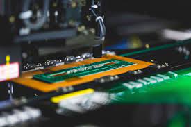
The first step in manufacturing high frequency PCBs is selecting the appropriate substrate material. Materials like PTFE (Polytetrafluoroethylene), FR-4 (Flame Retardant-4), or specialized ceramics are commonly used due to their low dielectric loss and high thermal stability at high frequencies.
Once the substrate material is chosen, it undergoes a process known as copper cladding. Thin layers of copper foil are laminated onto both sides of the substrate using heat and pressure. The thickness and quality of the copper layer are critical for maintaining signal integrity. Holes for component mounting and interconnections are drilled into the board using precision drilling machines. These holes are then plated with copper to ensure electrical connectivity between layers.